Background
I have recently been studying how to introduce the Wishbone bus protocol into my Principles of Computer Composition course, so I took the opportunity to learn about the Wishbone protocol.
Bus
What is a bus? The bus is usually used to connect CPU and peripherals. For better compatibility and reusability, it is thought that a unified protocol can be designed, where the CPU implementation is the party that initiates the request (also known as master) and the peripheral implementation is the party that receives the request (also known as slave), so that if you want to add peripherals or replace the CPU implementation, it becomes simpler and reduces a lot of adaptation workload.
So, let’s think about what a bus protocol needs to include. For the CPU, the program will read and write memory, and reading and writing memory requires the following signals to be transferred to memory.
- address (
addr): for example, a 32-bit processor is a 32-bit address, or the width of the address line is calculated according to the size of the memory - data (
w_dataandr_data): write data and read data respectively, usually 32 or 64 bits wide, i.e. the amount of data that can be transferred in one clock cycle - read or write (
we): high means write, low means read - byte valid (
be): for example, to achieve a single-byte write, althoughw_datamay be 32 bits wide, but the actual write is one of the bytes
In addition to the content of the request, a valid signal is added to indicate that the CPU wants to send the request: high means send the request, low means don’t send the request. In many cases, the peripheral is slow and may not be able to process the request every cycle, so the peripheral can provide a ready signal: when valid=1 && ready=1, the request is sent and processed; when valid=1 && ready=0, it means the peripheral is not ready, so the CPU needs to keep valid=1, and when the peripheral is ready, the valid=1 && ready=1 request will take effect.
To briefly summarize the above requirements, we can get the list of signals on the master and slave side respectively. This time, we use _o for output and _i for input to get the signals on the master side (CPU side).
clock_i: clock inputvalid_o: high means master wants to send requestready_i: high means the slave is ready to process the requestaddr_o: the address that master wants to read or write towe_o: master wants to read or writedata_o: master wants to write the databe_o: master read/write byte enable, used to implement single byte write, etc.data_i: the data that the slave provides to the master for reading
In addition to the clock are input, the rest of the above signals input and output symmetry, you can get the slave side (peripheral side) of the signal.
clock_i: clock inputvalid_i: high means master wants to send requestready_o: high means the slave is ready to process the requestaddr_i: the address that master wants to read or write towe_i: master wants to read or writedata_i: the data that master wants to writebe_i: master read/write byte enable, used to implement single byte write, etc.data_o: the data that the slave provides to the master for reading
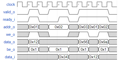
Based on the self-research bus we designed above, the following waveform can be plotted (with the master’s signal as an example).

acycle: at this timevalid_o=1 && ready_i=1means there is a request, at this timewe_o=1means it is a write operation and the write address isaddr_o=0x01and the data written isdata_o=0x12bcycle: at this pointvalid_o=0 && ready_i=0means nothing happenedccycle: at this timevalid_o=1 && ready_i=0means master wants to read data (we_o=0) from address 0x02 (addr_o=0x02), but slave does not accept it (ready_i=0)dcycle: at this pointvalid_o=1 && ready_i=1means there is a request, master reads data (we_o=0) from address 0x02 (addr_o=0x02), and the data read is 0x34 (data_i=0x34)ecycle: at this pointvalid_o=0 && ready_i=0means nothing happenedfcycle: at this timevalid_o=1 && ready_i=1means there is a request, master writes data (we_o=1) to address 0x03 (addr_o=0x03), the written data is 0x56 (data_i=0x56)gcycle: at this timevalid_o=1 && ready_i=1means there is a request, master reads data (we_o=0) from address 0x01 (addr_o=0x01), the data read is 0x12 (data_i=0x12)hcycle: at this pointvalid_o=1 && ready_i=1means there is a request, master writes data (we_o=1) to address 0x02 (addr_o=0x02), the data written is 0x9a (data_i=0x9a)
From the waveform above, several observations can be made.
- when the master wants to initiate a request, set
valid_o=1; when the slave can accept the request, setready_i=1; whenvalid_o=1 && ready_i=1, it is considered as one request - If the master initiates the request and the slave cannot receive the request, i.e.
valid_o=1 && ready_i=0, the master should keepaddr_o,we_o,data_oandbe_ounchanged until the request ends - When the master does not initiate a request, i.e.
valid_o=0, the signals on the bus are considered invalid and should not be processed; for read operations, the data ondata_iis valid only whenvalid_o=1 && ready_i=1. - The request can occur for multiple consecutive cycles, i.e.
valid_o=1 && ready_i=1is equal to one for multiple consecutive cycles, which is the ideal situation to achieve the highest transmission speed of the bus
Wishbone Classic Standard
First let’s look at the simplest version of Wishbone, Wishbone Classic Standard, which is very similar to the above self-research bus, so let’s take a look at its signals, such as the master side (CPU side).
CLK_I: clock input, i.e.clock_iin the self-developed busSTB_O: high means master wants to send a request, i.e.valid_oin the self-research busACK_I: High means the slave is processing the request, i.e.ready_iin the self-research busADR_O: the address that master wants to read or write, i.e.addr_oin the self-research busWE_O: whether master wants to read or write, i.e.we_oin the self-study busDAT_O: the data that master wants to write, i.e.data_oin the self-research busSEL_O: master’s byte read/write enable, i.e.be_oin the self-study busDAT_I: data read by master from slave, i.e.data_iin the self-study busCYC_O: enable signal of the bus, no corresponding self-research bus signal
There are also some optional signals, so I won’t go into them here. As you can see, except for the last one CYC_O, the other signals are actually the self-developed bus we just designed. The CYC_O can be considered as the master wants to occupy the slave’s bus interface, and in common usage scenarios, it is directly considered as CYC_O=STB_O. It is used for the following purposes
- to occupy the bus interface of the slave and not allow other masters to access it
- simplify the implementation of interconnect
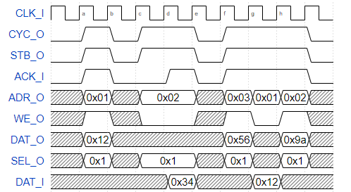
By replacing the waveform of the self-researched bus above with Wishbone Classic Standard, we get.

Wishbone Classic Pipelined
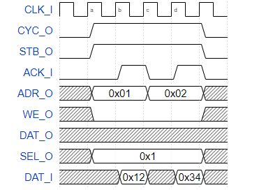
The Wishbone Classic Standard protocol above is very simple, but it runs into a problem: suppose the implementation is an SRAM controller that has a one-cycle delay for read operations, i.e., the address is given in one cycle and the result is not available until the next cycle. In Wishbone Classic Standard, the following waveform would appear.

acycle: master gives the read address 0x01, then the SRAM controller starts reading, but the data is not read back yet, soACK_I=0.bcycle: SRAM finishes reading, put the read data 0x12 inDAT_Iand setACK_I=1.ccycle: master gives the next read address 0x02, SRAM has to start reading againdcycle: the SRAM finishes the second read, puts the read data 0x34 inDAT_Iand setsACK_I=1.
From the waveform, there is no problem with the function, but only one read operation can be performed every two cycles, which does not bring out the highest performance. So how to solve this problem? We give the first address in a cycle and get the first data in b cycle, then if we can give the second address in b cycle, we can get the second data in c cycle. In this way, a pipelined read operation can be performed once per cycle. However, Wishbone Classic Standard requires that the first request is not finished by the b cycle, so we need to modify the protocol to implement a pipelined request.
The idea is simple: since Wishbone Classic Standard considers the first request to be pending at the b cycle, let the first request be completed earlier in the a cycle, except that its data will not be available until the b cycle. In fact, a read operation at this time can be considered as divided into two parts: first, the master sends a read request to the slave, which is completed in the a cycle; then the slave sends the result of the read to the master, which is completed in the b cycle. To achieve this, we make the following changes.
- Add
STALL_Isignal:CYC_O=1 && STB_O=1 && STALL_I=0to indicate a read request - Modify the meaning of
ACK_Isignal:CYC_O=1 && STB_O=1 && ACK_I=1means one read response
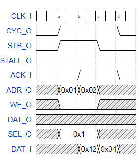
With the above modifications, we have the Wishbone Classic Pipelined bus protocol. The waveforms of the two consecutive read operations above are shown below.

acycle: master requests read address 0x01, slave receives read request (STALL_O=0)bcycle: slave returns read request result 0x12 and setsACK_I=1; at the same time master requests read address 0x02, slave receives read request (STALL_O=0)ccycle: slave returns the result of read request 0x34 and setsACK_I=1; master does not initiate request anymore and setsSTB_O=0dcycle: all requests complete, master setsCYC_O=0
This way we have implemented a slave that performs one read operation per cycle.